Complete ASIC Design Flow Explained: From Specification to Tapeout
- ASIC Design Flow Explained
Introduction
Application-Specific Integrated Circuits (ASICs) power modern smartphones, AI accelerators, automotive systems, networking equipment, and data centers. Behind every successful chip lies a structured development process known as the ASIC Design Flow.
For students and engineers entering the semiconductor industry, understanding the complete ASIC design flow is essential because it connects all major VLSI domains, including RTL Design, Verification, Physical Design, Timing Analysis, and Manufacturing.
In this guide, we explain each stage of the ASIC design cycle from specification to tapeout.
What Is an ASIC?
ASIC Design Flow Explained.
An ASIC (Application-Specific Integrated Circuit) is a custom-designed semiconductor chip optimized for a specific application.
Examples include:
- AI Accelerators
- Smartphone Processors
- Networking Switches
- Automotive Controllers
- SSD Controllers
Unlike general-purpose processors, ASICs are designed for dedicated functionality and optimized performance.
Asic design flow explained.
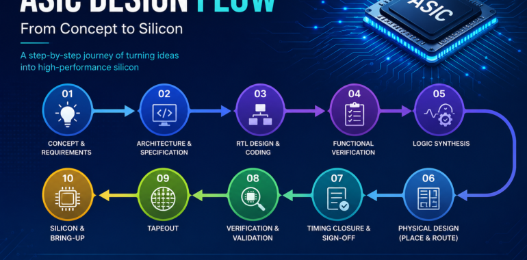
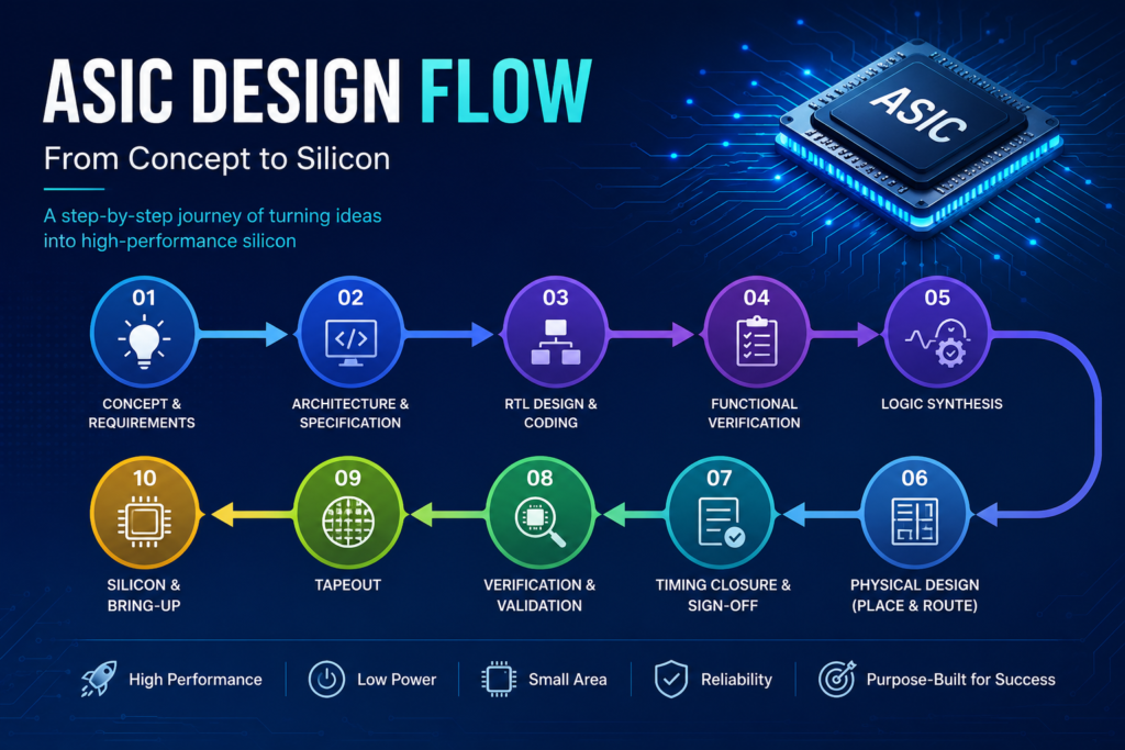
Overview of the ASIC Design Flow
The ASIC design flow consists of:
- Specification
- Architecture Design
- RTL Design
- Functional Verification
- Synthesis
- Design for Testability (DFT)
- Floorplanning
- Placement
- Clock Tree Synthesis
- Routing
- Static Timing Analysis
- Physical Verification
- Signoff
- Tapeout
Each stage contributes to ensuring the chip functions correctly and can be manufactured successfully.
1. Specification Phase
Every ASIC project begins with requirements gathering.
Engineers define:
- Functional requirements
- Performance targets
- Power constraints
- Area goals
- Cost limitations
This document serves as the foundation for the entire project.
2. Architecture Design
System architects determine:
- Processing blocks
- Memory hierarchy
- Bus interfaces
- Pipeline structure
- Clocking strategy
Architecture decisions have a major impact on performance and power consumption.
3. RTL Design
RTL engineers convert architecture into hardware description languages.
Common languages:
- Verilog
- SystemVerilog
RTL design includes:
- FSM Development
- Data Path Design
- Protocol Controllers
- Interface Logic
RTL is the heart of Frontend VLSI.
4. Functional Verification
Verification ensures RTL behaves according to specification.
Verification activities include:
- Simulation
- Assertions
- Coverage Analysis
- UVM Testbenches
- Debugging
Verification often consumes over 60% of the design cycle.
5. Logic Synthesis
Synthesis converts RTL into gate-level netlists.
Goals:
- Meet timing
- Reduce area
- Minimize power
Output:
- Gate-Level Netlist
6. Design for Testability (DFT)
DFT improves manufacturing test coverage.
Common techniques:
- Scan Chains
- Boundary Scan
- BIST
- JTAG
DFT helps detect manufacturing defects.
7. Floorplanning
Backend engineers define:
- Macro placement
- Memory locations
- Power grid
- I/O placement
A good floorplan improves timing and routing efficiency.
8. Placement
Standard cells are positioned inside the chip area.
Objectives:
- Minimize congestion
- Improve timing
- Optimize utilization
9. Clock Tree Synthesis (CTS)
CTS distributes clock signals across the chip.
Goals:
- Reduce skew
- Control latency
- Improve timing reliability
10. Routing
Routing connects all placed cells using metal layers.
Routing must satisfy:
- Timing constraints
- Design rules
- Signal integrity requirements
11. Static Timing Analysis (STA)
STA verifies timing without simulation.
Key checks:
- Setup Time
- Hold Time
- Clock Skew
- Timing Closure
12. Physical Verification
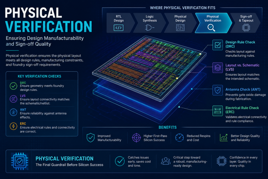
ASIC Design Flow Explained.
Verification before manufacturing includes:
- DRC
- LVS
- ERC
These checks ensure layout correctness.
13. Signoff
Signoff confirms:
- Timing closure
- Power integrity
- Physical verification
- Reliability metrics
Only signoff-approved designs proceed further.
14. Tapeout
Tapeout is the final stage.
Design data is sent to the semiconductor foundry for fabrication.
This marks the transition from design to manufacturing.
Career Opportunities Across the ASIC Flow
Frontend Roles:
- RTL Design Engineer
- Verification Engineer
- FPGA Engineer
Backend Roles:
- Physical Design Engineer
- STA Engineer
- DFT Engineer
System Roles:
- SoC Engineer
- Architecture Engineer
Conclusion
The ASIC design flow is a structured process that transforms a concept into silicon. Understanding each stage helps engineers appreciate how Frontend and Backend VLSI work together to build modern semiconductor products.
Whether your goal is RTL Design, Verification, Physical Design, or Architecture, mastering the ASIC flow provides the foundation for a successful VLSI career.
VLSI INSIGHTS -socials
Follow VLSI Insights linkedin https://www.linkedin.com/company/104170744/admin/page-posts/published/
follow Youtube – https://www.youtube.com/@VLSIInsights9
Follow Instagram – https://www.instagram.com/vlsiinsights/