What Are Chiplets? How Chiplet-Based Design Is Transforming the Semiconductor Industry in 2026
What Are Chiplets ? Future of Chip Design in 2026 | VLSI Insights
The semiconductor industry is evolving rapidly, driven by the explosive growth of Artificial Intelligence (AI), High-Performance Computing (HPC), cloud infrastructure, and edge devices. As demand for more powerful and efficient chips increases, traditional monolithic chip designs are reaching their physical and economic limits.
To overcome these challenges, semiconductor companies are increasingly adopting Chiplet Design—a revolutionary approach that breaks a large chip into multiple smaller dies called chiplets. This architectural shift is transforming how modern processors, AI accelerators, and data center chips are designed and manufactured.
In this article, we’ll explore what chiplets are, how chiplet-based design works, and why this technology is becoming one of the most important trends in the semiconductor industry in 2026.
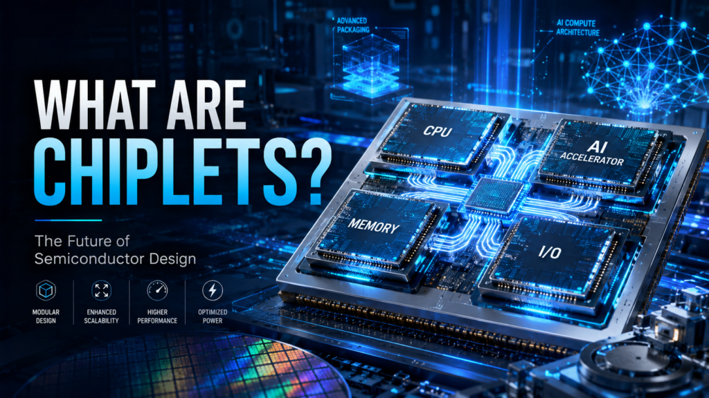
What Are Chiplets?
A chiplet is a small semiconductor die designed to perform a specific function within a larger integrated system.
Instead of building a complete System-on-Chip (SoC) as one large piece of silicon, engineers divide the design into multiple specialized chiplets and connect them together inside a single package.
Each chiplet may handle a different function such as:
- CPU Processing
- Memory Control
- Input/Output (I/O)
- AI Acceleration
- Graphics Processing
Together, these chiplets function as a single high-performance processor.
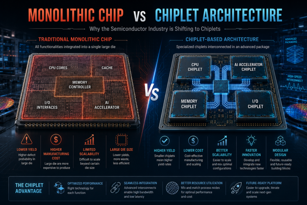
Why Traditional Monolithic Chips Are Facing Challenges
For decades, semiconductor companies relied on monolithic chip design, where all functions are integrated into a single silicon die.
While this approach has worked well, modern chips now contain billions of transistors, creating several challenges:
Increasing Manufacturing Costs
Advanced process nodes such as 3nm and 2nm require enormous investments in fabrication technology.
Lower Manufacturing Yield
A defect anywhere on a large die can cause the entire chip to fail, increasing production costs.
Limited Scalability
Adding more functionality to a monolithic design becomes increasingly difficult as chip complexity grows.
These challenges have encouraged the industry to explore new design methodologies.
What Is Chiplet-Based Design?
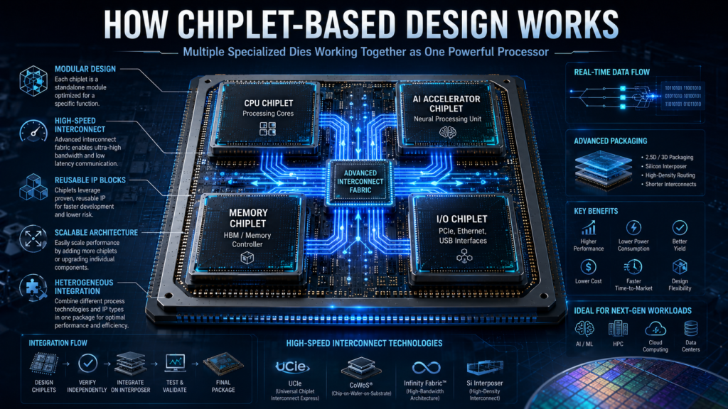
Chiplet-based design separates major functions into independent silicon dies.
A modern processor package may contain:
CPU Chiplet
Contains processing cores and cache memory.
I/O Chiplet
Handles PCIe, USB, Ethernet, and external communication interfaces.
AI Accelerator Chiplet
Performs machine learning and AI computations.
Memory Chiplet
Provides high-speed memory access and storage functions.
These chiplets are connected through advanced packaging and high-speed interconnect technologies, allowing them to operate as a unified system.
Why Is Chiplet Design Becoming Popular in 2026?
Several industry trends are accelerating chiplet adoption.
1. The Rise of Artificial Intelligence
AI workloads require enormous computing power and memory bandwidth.
Chiplet architectures allow semiconductor companies to combine specialized compute engines, memory systems, and AI accelerators efficiently.
This flexibility makes chiplets ideal for AI-focused processors.
2. Better Manufacturing Efficiency
Smaller chiplets achieve higher manufacturing yields than large monolithic dies.
If one chiplet contains a defect, only that chiplet needs replacement instead of discarding the entire processor.
3. Faster Product Development
Chiplets can be reused across multiple product families.
A company can use the same I/O chiplet in desktop processors, server processors, and AI accelerators, significantly reducing development time.
4. Cost Optimization
Different chiplets can be manufactured using different process technologies.
For example:
- CPU Chiplet → 3nm
- I/O Chiplet → 7nm
- Analog Chiplet → 14nm
This reduces manufacturing costs while maintaining performance.
Key Benefits of Chiplet Design
Improved Scalability
Chiplets make it easier to increase processor performance by adding more specialized dies.
Higher Manufacturing Yield
Smaller dies have fewer defects and higher production success rates.
Lower Development Costs
Reusable chiplets reduce engineering effort and shorten product development cycles.
Better Performance per Dollar
Chiplets allow companies to achieve higher performance without dramatically increasing manufacturing costs.
Heterogeneous Integration
Different technologies can be integrated into a single package, creating highly optimized semiconductor solutions.
What Is UCIe and Why Does It Matter?
One of the biggest challenges in chiplet design is enabling fast communication between chiplets.
This is where UCIe (Universal Chiplet Interconnect Express) plays an important role.
UCIe is an industry-standard interconnect protocol designed to allow chiplets from different vendors to communicate efficiently.
Benefits of UCIe include:
- High-speed communication
- Lower latency
- Vendor interoperability
- Simplified chiplet ecosystem development
Many leading semiconductor companies are supporting UCIe as the future standard for chiplet connectivity.
How Chiplets Are Powering AI Chips
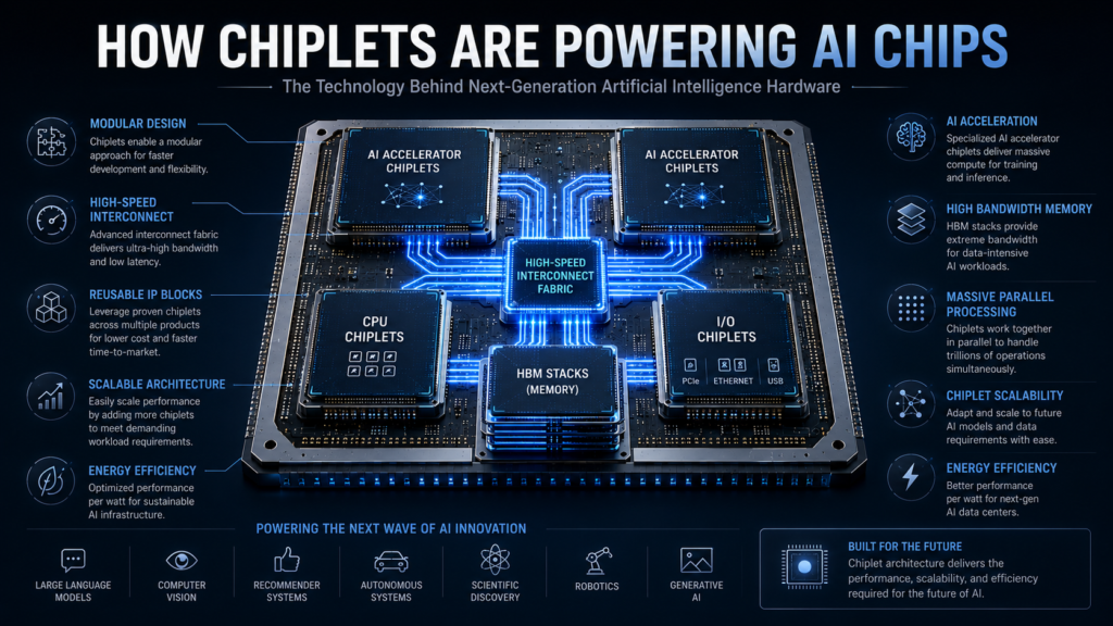
Artificial Intelligence is currently the largest growth driver in the semiconductor industry.
Modern AI processors require:
- Massive computational power
- High-bandwidth memory
- Efficient data movement
- Scalable architectures
Chiplets enable designers to combine multiple AI accelerators, memory modules, and compute engines within a single package.
This approach improves:
- Performance
- Energy efficiency
- Scalability
making chiplets essential for next-generation AI hardware.
Impact of Chiplets on VLSI Engineers
As chiplet adoption increases, VLSI engineers will need to develop new skills.
Important areas include:
RTL Design
Developing reusable IP blocks that can function as independent chiplets.
Functional Verification
Verifying communication between multiple chiplets and subsystems.
System Architecture
Designing scalable multi-die semiconductor systems.
Advanced Packaging
Understanding 2.5D and 3D integration technologies.
High-Speed Interconnects
Working with standards such as UCIe and advanced communication protocols.
These skills are expected to become increasingly valuable in the coming years.
Challenges of Chiplet-Based Design
Despite its advantages, chiplet technology introduces new engineering challenges.
Interconnect Complexity
Communication between chiplets must be reliable, fast, and power efficient.
Verification Challenges
Multiple dies create additional validation and testing requirements.
Thermal Management
Packing several dies into a single package can generate significant heat.
Advanced cooling and packaging solutions are required to maintain performance and reliability.
The Future of Chiplets in the Semiconductor Industry
Industry experts believe chiplets will become a standard design methodology for:
- AI Accelerators
- Data Center Processors
- GPUs
- Automotive Electronics
- Edge Computing Devices
- High-Performance Computing Systems
As AI applications continue expanding, chiplet-based architectures will play a critical role in delivering higher performance while controlling manufacturing costs.
The future of semiconductor innovation is no longer focused solely on shrinking transistors—it is increasingly focused on intelligently integrating specialized chiplets into powerful systems.
Conclusion
Chiplet design is transforming the semiconductor industry by providing a scalable, cost-effective alternative to traditional monolithic chips.
With benefits such as improved manufacturing yield, lower costs, better scalability, and support for AI workloads, chiplets are becoming a cornerstone of modern semiconductor architecture.
For students, engineers, and professionals working in VLSI and semiconductor design, understanding chiplet technology is becoming increasingly important as the industry moves toward a chiplet-driven future.
Frequently Asked Questions (FAQ)
What is a chiplet?
A chiplet is a small semiconductor die designed to perform a specific function within a larger chip package. Multiple chiplets work together to create a complete processor or system.
Why are chiplets important?
Chiplets improve manufacturing yield, reduce costs, and provide greater flexibility compared to traditional monolithic chip designs.
What is UCIe?
UCIe (Universal Chiplet Interconnect Express) is an industry-standard communication protocol that enables high-speed connectivity between chiplets.
Which companies are using chiplet technology?
Major semiconductor companies including AMD, Intel, NVIDIA, Broadcom, and TSMC are actively investing in chiplet-based architectures.
Are chiplets the future of semiconductor design?
Yes. Chiplets are widely considered one of the most important semiconductor innovations because they enable scalable, high-performance designs for AI, HPC, and next-generation computing applications.
Key Takeaways
- Chiplets break large processors into smaller specialized dies for improved flexibility and scalability.
- Chiplet-based design helps reduce manufacturing costs while improving production yield.
- AI, data centers, and high-performance computing are accelerating chiplet adoption across the semiconductor industry.
- UCIe is emerging as the key standard for high-speed communication between chiplets.
- Major semiconductor companies such as AMD, Intel, NVIDIA, and TSMC are investing heavily in chiplet architectures.
- Chiplet technology is expected to play a central role in the future of AI chips and next-generation semiconductor innovation.