Vlsi Insights

RTL Design vs Design Verification: Which VLSI Career Path Is Right for Your Growth in 2026?

Home/

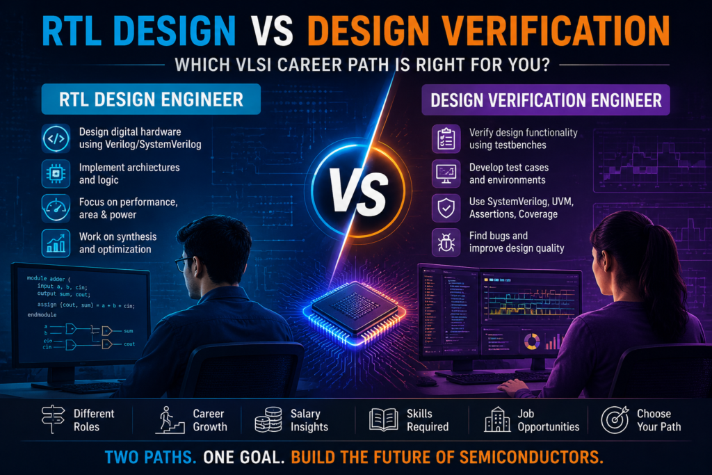
(RTL Design vs Design Verification.)

The semiconductor industry is growing rapidly, creating thousands of opportunities for engineers who want to build a career in VLSI.

However, one of the biggest questions every VLSI beginner faces is:

“Should I choose RTL Design or Design Verification?”

Both RTL Design and Design Verification are important parts of the VLSI Frontend Design Flow. Both require strong knowledge of digital electronics, Verilog, and hardware concepts.

But the roles, responsibilities, skills, and career paths are completely different.

In this article, we will understand:

  • What is RTL Design?
  • What is Design Verification?
  • Difference between RTL Design and Verification
  • Skills required for each role
  • Career opportunities
  • Salary comparison
  • Which VLSI domain is better for freshers in 2026?

What Is RTL Design in VLSI?

RTL (Register Transfer Level) Design is the process of converting hardware specifications into a digital hardware description using Hardware Description Languages (HDLs) like Verilog and SystemVerilog.

An RTL Design Engineer creates the actual hardware logic that becomes part of a semiconductor chip.

RTL designers work on developing:

  • Processor blocks
  • Controllers
  • Communication modules
  • Memory interfaces
  • Digital IP blocks

Role of an RTL Design Engineer

An RTL Design Engineer is responsible for:

  • Understanding hardware specifications
  • Designing digital circuits
  • Writing synthesizable RTL code
  • Implementing logic using Verilog/SystemVerilog
  • Performing simulations
  • Debugging design issues
  • Working with synthesis and physical design teams

For example, if a company wants to design a communication controller inside a chip, the RTL engineer converts the required functionality into hardware logic using RTL coding.


What Is Design Verification in VLSI?

Design Verification is the process of ensuring that a hardware design works correctly according to the given specifications.

While RTL engineers create the hardware, verification engineers test and validate that hardware.

The main objective of verification is:

“Finding bugs before the chip reaches manufacturing.”

Design Verification Engineers work on:

  • Creating verification environments
  • Developing testbenches
  • Running simulations
  • Finding functional bugs
  • Debugging failures
  • Ensuring design quality

RTL Design vs Design Verification: Complete Comparison

(RTL Design vs Design Verification.)

ParameterRTL DesignDesign Verification
Main PurposeCreating hardware logicTesting hardware functionality
Primary SkillRTL codingVerification methodology
LanguagesVerilog, SystemVerilogSystemVerilog, UVM
Work FocusDesign implementationBug detection
CreativityHardware architectureTest strategy development
DebuggingDesign issuesFunctional failures
ToolsVivado, Design Compiler, QuestaQuesta, VCS, Verdi
Career ScopeExcellentExcellent

Skills Required to Become an RTL Design Engineer

1. Strong Digital Electronics Foundation

Every RTL engineer must understand:

  • Logic gates
  • Boolean algebra
  • Combinational circuits
  • Sequential circuits
  • Flip-flops
  • Counters
  • Registers
  • FSM Design

2. Verilog and SystemVerilog

Important concepts include:

  • Modules
  • Data types
  • Always blocks
  • Operators
  • Blocking and non-blocking assignments
  • RTL coding practices

3. Hardware Design Concepts

A good RTL engineer should understand:

  • Clock design
  • Reset techniques
  • Timing concepts
  • Synthesis
  • Hardware architecture

Skills Required to Become a Design Verification Engineer

(RTL Design vs Design Verification.)

1. Digital Electronics

Verification engineers also require strong fundamentals in:

  • Logic circuits
  • FSM
  • Timing concepts
  • Protocol understanding

2. SystemVerilog Programming

Important topics include:

  • Object-oriented programming
  • Classes
  • Randomization
  • Interfaces
  • Testbench development

3. UVM Methodology

Modern semiconductor companies use UVM for verification.

Important concepts:

  • UVM Components
  • Sequence
  • Driver
  • Monitor
  • Scoreboard
  • Functional Coverage

RTL Design vs Verification: Which Career Has Better Scope?

The semiconductor industry is expanding because of:

  • Artificial Intelligence chips
  • Automotive electronics
  • IoT devices
  • Advanced processors
  • Semiconductor manufacturing growth

Both RTL Design and Verification engineers are highly demanded because every chip requires:

  1. Hardware creation
  2. Hardware validation

Without RTL Design, chips cannot be created.

Without Verification, chips cannot be trusted.


Salary Comparison of RTL Design and Verification Engineers in India

(RTL Design vs Design Verification.)

RTL Design Engineer Salary

Freshers:

₹5 LPA – ₹12 LPA

Experienced Engineers:

₹15 LPA – ₹40+ LPA

Design Verification Engineer Salary

Freshers:

₹5 LPA – ₹10 LPA

Experienced Engineers:

₹15 LPA – ₹35+ LPA

Salary depends on:

  • Technical skills
  • Company
  • Projects
  • Interview performance
  • Practical experience

Which VLSI Career Path Is Better for Freshers?

There is no single best option.

The right choice depends on your interest.

Choose RTL Design If You Like:

  • Creating hardware
  • Digital logic
  • Circuit implementation
  • Architecture development
  • Writing RTL code

Choose Verification If You Like:

  • Finding bugs
  • Debugging problems
  • Testing designs
  • Analytical thinking
  • Creating test scenarios

Learning Roadmap for VLSI Beginners

(RTL Design vs Design Verification.)

Common Foundation

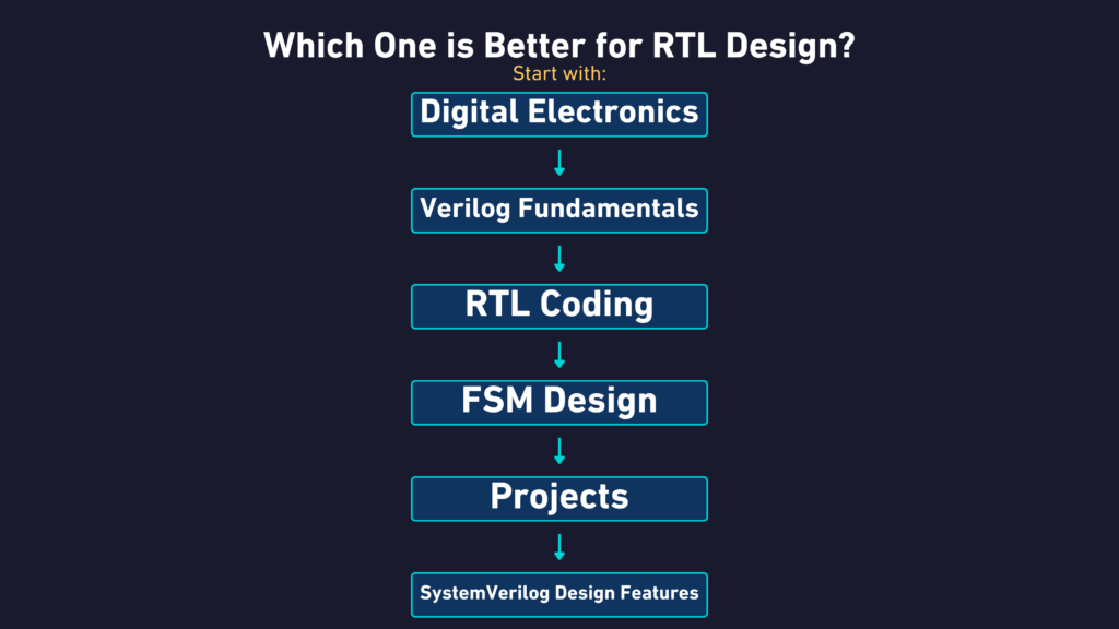
Step 1: Learn Digital Electronics

Step 2: Learn Verilog Programming

Step 3: Understand VLSI Design Flow

Step 4: Learn SystemVerilog Basics

After this, choose your specialization.

RTL Design Roadmap

Digital Electronics

Verilog

RTL Coding

FSM Design

Synthesis

Static Timing Analysis

Verification Roadmap

Digital Electronics

Verilog

SystemVerilog

Testbench Development

UVM

Functional Verification


Important Projects to Build Your VLSI Portfolio

RTL Design Projects

  • ALU Design
  • FIFO Design
  • UART Controller
  • Traffic Light Controller
  • APB Protocol Design

Verification Projects

  • FIFO Verification Environment
  • UART Verification using SystemVerilog
  • Memory Verification
  • APB Protocol Verification

Projects demonstrate practical skills and improve your chances during interviews.


Common Mistake Students Make While Learning VLSI

Many beginners directly start learning Verilog or SystemVerilog without understanding digital electronics fundamentals.

A successful VLSI career requires:

  • Strong fundamentals
  • Practical coding skills
  • Industry-relevant projects
  • Interview preparation

Learning tools alone is not enough. Understanding hardware concepts is the key.


How VLSI Insights Helps Students Build Their VLSI Career

At VLSI Insights, students learn industry-focused VLSI fundamentals through practical training.

The program covers:

  • Digital Electronics
  • Verilog RTL Design
  • SystemVerilog Basics
  • VLSI Projects
  • Verification Concepts
  • Interview Preparation

The goal is to help students build job-ready semiconductor skills and understand real-world VLSI workflows.


Key Takeaways

  • RTL Design focuses on creating hardware logic.
  • Design Verification focuses on testing and validating hardware.
  • Both domains have strong career opportunities.
  • Digital Electronics is the foundation for both paths.
  • Verilog and SystemVerilog are essential skills.
  • Practical projects improve VLSI job readiness.

Frequently Asked Questions (FAQ)

(RTL Design vs Design Verification.)

1. Is RTL Design better than Verification?

Both RTL Design and Verification have excellent career opportunities. The better choice depends on your interest and skill set.

2. Which VLSI domain is best for freshers?

RTL Design and Verification both offer entry-level opportunities for freshers with strong fundamentals.

3. Is UVM required for VLSI Verification jobs?

Yes, UVM is an important skill for advanced verification roles.

4. Can ECE students build a career in VLSI?

Yes, ECE graduates can enter VLSI by learning digital electronics, Verilog, SystemVerilog, and practical projects.

5. Which language is required for RTL Design?

Verilog and SystemVerilog are the primary languages used for RTL development.


External References

external links:


Links

Best Skills for RTL Design Engineers in 2026: Complete Career Roadmap

Frontend vs Backend VLSI: Which Career Path Is Better in 2026?

vlsi career roadmap 2026

https://images.openai.com/static-rsc-4/LT_IVX_9ts52EaBPIBibVe4lL1Rm2h9FS3Xhwgdp8AfNxG_s8cY3dDHMvp5UEReLs7aWrwfuN_llyZrdno07ySlkec6O4LVaDj21uHcw2fhe1ZwjdbXlzCAvXWCh0JyCrj5TAN6XS3vJxj8Q8etXM3J3T4YGh35607HV9ghX2n6TxzgM21Ntl1cGVpzb2FuN?purpose=fullsize

The semiconductor industry is entering one of the most exciting phases in history.

From Artificial Intelligence processors and autonomous vehicles to smartphones, cloud computing, and advanced electronics, every modern technology depends on semiconductor chips.

According to industry reports, global semiconductor demand is expected to continue growing rapidly due to AI, automotive electronics, IoT, and high-performance computing.

For Electronics and Communication Engineering (ECE) students, this growth has created massive opportunities in the VLSI domain.

But many students have one major question:

“How do I start my career in VLSI and become a VLSI engineer?”

The answer is not learning random tools or watching scattered tutorials.

A successful VLSI career requires a structured roadmap covering:

  • Digital Electronics fundamentals
  • Verilog and RTL Design
  • SystemVerilog
  • Design Verification
  • UVM methodology
  • VLSI projects
  • Industry tools
  • Interview preparation

This complete VLSI Career Roadmap 2026 will guide beginners, fresh graduates, and aspiring chip designers step-by-step.


What is VLSI?

VLSI stands for Very Large Scale Integration.

It is the process of designing and manufacturing integrated circuits (ICs) by combining millions or even billions of transistors onto a single semiconductor chip.

Modern processors, GPUs, memory chips, and AI accelerators are created using VLSI technology.

A VLSI engineer works on different stages of chip development including:

  • Architecture design
  • RTL coding
  • Functional verification
  • Physical design
  • Timing analysis
  • Semiconductor manufacturing support

Learn more about semiconductor technology from:

External Reference:
Semiconductor Industry Association


Why Choose VLSI as a Career in 2026?

vlsi career roadmap 2026

The semiconductor ecosystem is expanding because of:

1. Artificial Intelligence Growth

AI applications require powerful processors and specialized AI chips.

Companies are investing heavily in:

  • AI accelerators
  • GPUs
  • Neural processing units
  • High-performance computing chips

2. Semiconductor Manufacturing Growth

Countries worldwide are investing in semiconductor manufacturing and design ecosystems.

India is also becoming an important semiconductor design hub.

Government initiatives like the India Semiconductor Mission are supporting semiconductor development.

External Reference:

India Semiconductor Mission Official Website

3. High Demand for Skilled VLSI Engineers

The industry requires engineers with expertise in:

  • RTL Design
  • Verification
  • SystemVerilog
  • UVM
  • Physical Design
  • Semiconductor tools

Who Can Build a Career in VLSI?

VLSI is suitable for:

✅ Electronics Engineering students
✅ Electrical Engineering students
✅ Computer Engineering students interested in hardware
✅ Fresh graduates
✅ Working professionals looking to transition into semiconductor careers

Common educational backgrounds:

  • B.Tech ECE
  • B.Tech EEE
  • B.Tech Electronics
  • M.Tech VLSI Design

Different Career Paths in VLSI

vlsi career roadmap 2026

A common mistake beginners make is thinking VLSI means only chip designing.

The semiconductor industry has multiple career paths.

https://images.openai.com/static-rsc-4/Hh-6zHGgtusCSJrP7s9ucrWXDF4FOJf-L4I9Fj1_0gqHn0D8llE0OZJNtLSQCswyzLNrXMYrymc8CsLh9gWtlaJ5KIjT05WNCcvMufKMTYgZugWMRqG9bxDx18_-E_cCOAGM1J9JhWVccHHHCl90cOoQFrmumurTQG6FlJ9tNWgwjvQGlnrTgMUh9VRkI8Hg?purpose=fullsize
https://images.openai.com/static-rsc-4/2gtbtAdpneQr0yBFiCYmPD444a0XeIgBLYDMGPEd-tikwNgZq0FW03_5AwroScKWFbn_aKshndslSJQHkXxjt4BuCHwn5RxsXt4Gyjsw_gGrV_UcP-t7X7ot0wHbFj2bzGCDEMhak2ybPEaUQwlHbOVBfKoxbu30yjnS3u-vpLV0387fXMo2eTmt2NR_QbV2?purpose=fullsize
https://images.openai.com/static-rsc-4/EpGo8SbRgR3SiNGPDyy3nKfQhTUvFvksHkk_20mPHqLQCKgdinLhyALIpDFUrglQVsaQZVwOvTxjIbtQ6Fj_19HYSu8qA1D-CCvhvlv1NWyFX49mbPJjC-yrvpqUesMhWf1OOt5LBr6qAfo2lgRHo5V5rUKB1bUy61QUFHQ6mPBDkjcMDvk25-hfjmftFLEs?purpose=fullsize

5

1. RTL Design Engineer

RTL engineers convert hardware architecture into synthesizable code.

Main skills:

  • Digital Electronics
  • Verilog
  • SystemVerilog
  • RTL coding
  • FSM design
  • Simulation

Typical projects:

  • Processor blocks
  • Controllers
  • Communication modules

2. Design Verification Engineer

Verification engineers ensure that the designed chip works correctly.

They find bugs before manufacturing.

Skills required:

  • SystemVerilog
  • Testbench development
  • Assertions
  • Coverage
  • UVM

Verification is one of the most popular entry paths for freshers.


3. Physical Design Engineer

Physical design focuses on converting RTL into a physical chip layout.

Skills:

  • Floor planning
  • Placement
  • Clock Tree Synthesis
  • Routing
  • Static Timing Analysis

4. Analog Design Engineer

Analog engineers design circuits involving:

  • Amplifiers
  • ADC/DAC
  • PLL
  • Power management circuits

Complete VLSI Career Roadmap 2026 (Beginner to Job Ready)

vlsi career roadmap 2026

https://images.openai.com/static-rsc-4/Io6OMnW9uHeUiL6WSilhKJLIakQ-vKLc6vz5MgONZXpKml9VLbByLGEyOlYAvaYJt4mv_mVoXsITuBVNIyVZ4sBMn7XH48v2ibAB-P08xCg4M0-I7jB3wSlFHPCe6Zu4GAhunOB5JUd88bubuBE_yIvjyDzhQPbbdenBeQv1Hv_dWxQ_IOIBY0uduy2afDPt?purpose=fullsize
https://images.openai.com/static-rsc-4/9DixKayRjwDa9xD6yBlR2iApQybM0eLkpLQSF2NTKzlB9_62RV5givAU1QtgQksL-TVeCHx85IedY9EWEj6UrL3fBs-DuFUhxSJ6j0v_nyT5RobhGnMNiQTZOMx8vV3_duQIgh0u3ndV4MNr9kMgHY9Gayj2FpcmIu_GF9EtpLEAG_SX5dhP1EU9EhxegdDq?purpose=fullsize
https://images.openai.com/static-rsc-4/wGYyIy16VF5H0S4TAyaEI1NVG8HHyGKFq_OpT7L8dBUaDFKffVa9oGVV9bWcx0_QGQwrFKwJNesiTmYCQfnagJpPjEr9Nr1wHLgUWPqEcFhypw8yzVaOVy0D9wdmk3QaIXVBDzrJD-PsKklNkFFakn7soD1r4HbAL18EBbb71IE9x6kcm54dsUgQb2jtUqj5?purpose=fullsize

5

Stage 1: Learn Digital Electronics Fundamentals

Duration:
4–6 weeks

Digital electronics is the foundation of VLSI.

You should understand:

Number Systems

  • Binary
  • Decimal
  • Hexadecimal
  • 1’s complement
  • 2’s complement

Combinational Circuits

Learn:

  • Multiplexer
  • Decoder
  • Encoder
  • Adders
  • Subtractors

Sequential Circuits

Important topics:

  • Flip flops
  • Registers
  • Counters
  • FSM Design

Without strong digital fundamentals, advanced VLSI concepts become difficult.


Stage 2: Learn Verilog HDL

Duration:
4–6 weeks

Verilog is used to describe hardware behavior.

Important concepts:

  • Modules
  • Ports
  • Data types
  • Operators
  • Always blocks
  • Testbench
  • Simulation

Projects:

  • ALU Design
  • FIFO
  • UART
  • Traffic Controller

Stage 3: Learn SystemVerilog

Duration:
4 weeks

SystemVerilog improves hardware verification capabilities.

Learn:

  • Classes
  • Objects
  • Interfaces
  • Randomization
  • Assertions
  • Functional coverage

Stage 4: Learn Verification Methodology (UVM)

Duration:
4–8 weeks

UVM is widely used in semiconductor companies for verification.

Topics:

  • UVM architecture
  • Sequence
  • Driver
  • Monitor
  • Scoreboard
  • Environment

External Reference:

Accellera UVM Standard


Skills Required to Become a VLSI Engineer

Technical Skills

SkillImportance
Digital Electronics⭐⭐⭐⭐⭐
Verilog⭐⭐⭐⭐⭐
SystemVerilog⭐⭐⭐⭐⭐
Linux⭐⭐⭐⭐
Scripting⭐⭐⭐
STA⭐⭐⭐⭐

VLSI Projects Every Student Should Build

Projects are extremely important because they demonstrate practical knowledge.

Recommended projects:

  1. ALU Design using Verilog
  2. FIFO Memory Controller
  3. UART Communication Module
  4. Traffic Light Controller using FSM
  5. APB Protocol Design
  6. RISC-V Processor Implementation
  7. Verification Environment using SystemVerilog

A strong project portfolio can significantly improve interview opportunities.


Common Mistakes Students Make While Learning VLSI

Mistake 1:

Learning tools without fundamentals

Mistake 2:

Only watching tutorials without implementation

Mistake 3:

Ignoring projects

Mistake 4:

Not preparing interview questions

Mistake 5:

Trying to learn every VLSI domain together

The right approach is:

Foundation → Coding → Projects → Specialization → Interview Preparation


VLSI Interview Preparation Roadmap

Companies usually evaluate:

Digital Electronics

Questions from:

  • Flip flops
  • FSM
  • Timing concepts
  • Logic circuits

Verilog

Questions:

  • Blocking vs non-blocking assignment
  • Always blocks
  • Synthesizable coding

Verification

Questions:

  • Testbench architecture
  • Coverage
  • Assertions
  • UVM concepts

Career Opportunities After Learning VLSI

Possible job roles:

  • RTL Design Engineer
  • Design Verification Engineer
  • Physical Design Engineer
  • FPGA Engineer
  • ASIC Engineer

Companies hiring semiconductor engineers include:

  • Intel Corporation
  • NVIDIA
  • Qualcomm
  • Texas Instruments
  • AMD

How VLSI Insights Helps Students Become Industry Ready

At VLSI Insights, our goal is to bridge the gap between academic learning and semiconductor industry requirements.

Our programs focus on:

✓ Digital Electronics Foundation
✓ RTL Design using Verilog
✓ SystemVerilog Fundamentals
✓ Verification Concepts
✓ Hands-on Projects
✓ Interview Preparation

If you are an ECE student looking to start your VLSI journey, building the right foundation is the first step.


Final Takeaway

vlsi-career-roadmap-2026

The VLSI industry offers one of the strongest career opportunities for electronics engineers in 2026.

However, success requires a structured learning path.

Follow this roadmap:

Digital Electronics → Verilog → SystemVerilog → Projects → Verification/RTL Specialization → Interviews

Start building your semiconductor career today.


Still confused ?

Want a personalized Vlsi career roadmap 2026?

Download our free beginner guide or connect with VLSI Insights experts.

[Get Free VLSI Career Roadmap]


RTL Design vs Design Verification.

Introduction

One of the most common questions among ECE students and aspiring VLSI professionals is:

“Should I choose RTL Design or Design Verification?”

Both career paths play critical roles in semiconductor development and offer excellent growth opportunities. However, the required skills, daily responsibilities, and career progression differ significantly.

This article compares RTL Design and Verification to help you make an informed career decision.

What Does an RTL Design Engineer Do?

RTL Design vs Design Verification: Which VLSI Career Path Is Right for You?

RTL Design Engineers convert architectural specifications into synthesizable hardware designs.

Their primary goal is to create efficient digital circuits using Verilog or SystemVerilog.

Typical responsibilities include:

  • RTL coding
  • FSM implementation
  • Design optimization
  • Power and area improvements
  • Synthesis support
  • Design reviews

Skills Required

  • Digital Electronics
  • Computer Architecture
  • Verilog
  • SystemVerilog
  • Synthesis Concepts
  • Timing Analysis Basics

Ideal For

Engineers who enjoy:

  • Hardware architecture
  • Problem solving
  • Circuit implementation
  • Logic optimization

What Does a Design Verification Engineer Do?

Verification Engineers validate whether the RTL design behaves according to specifications.

Their goal is to identify bugs before chip fabrication.

Typical responsibilities include:

  • Testbench development
  • Functional verification
  • UVM implementation
  • Coverage closure
  • Assertions
  • Debugging failures

Skills Required

  • Digital Electronics
  • SystemVerilog
  • Object-Oriented Programming
  • UVM Methodology
  • Assertions
  • Functional Coverage

Ideal For

Engineers who enjoy:

  • Debugging
  • Software-style programming
  • Test automation
  • Problem investigation

RTL Design vs Verification: Key Differences

(RTL Design vs Design Verification)

Coding Style

RTL Design:

  • Hardware-centric coding
  • Synthesizable RTL

Verification:

  • Testbench development
  • Object-oriented programming

Learning Curve

RTL Design:

  • Strong digital design fundamentals required

Verification:

  • Requires learning SystemVerilog OOP and UVM

Job Availability

Historically, verification teams are larger than design teams.

As a result, there are often more openings available in Design Verification compared to RTL Design.

Career Growth

RTL Design Path:

RTL Engineer → Senior RTL Engineer → Lead Designer → Architect

Verification Path:

Verification Engineer → Senior Verification Engineer → Verification Lead → Verification Manager

Which Domain Has Better Opportunities in 2026?

Both domains are expected to grow rapidly due to increasing semiconductor demand.

Choose RTL Design if you enjoy:

  • Hardware implementation
  • Logic design
  • Architecture development

Choose Verification if you enjoy:

  • Debugging
  • Programming concepts
  • Test automation
  • Finding design bugs

Can You Transition Between Domains?

Yes.

Many engineers start in Verification and later move into Design roles. Similarly, RTL engineers often gain verification experience while working on projects.

Having knowledge of both domains significantly increases career flexibility.

Recommended Learning Roadmap

For RTL Design

  1. Digital Electronics
  2. Verilog
  3. SystemVerilog
  4. FSM Design
  5. Synthesis Concepts
  6. RTL Projects

For Verification

  1. Digital Electronics
  2. Verilog
  3. SystemVerilog
  4. OOP Concepts
  5. Assertions
  6. UVM
  7. Verification Projects

Conclusion

There is no universally better choice between RTL Design and Design Verification. The right path depends on your interests, strengths, and long-term goals.

If you enjoy creating hardware, RTL Design may be the ideal fit. If you enjoy debugging, automation, and verification methodologies, Verification can offer an exciting and rewarding career.

Regardless of the path you choose, building strong fundamentals and gaining hands-on project experience are the keys to success in the semiconductor industry.

Frequently Asked Questions (FAQs)

1. What is the difference between an RTL Design Engineer and a Design Verification Engineer?

An RTL Design Engineer is responsible for creating digital hardware designs using Verilog or SystemVerilog based on design specifications. A Design Verification Engineer validates those designs by developing testbenches, running simulations, and identifying functional bugs before chip fabrication.

2. Which is better: RTL Design or Design Verification?

Neither role is universally better. RTL Design is ideal for engineers interested in hardware architecture and digital circuit implementation, while Design Verification is better suited for those who enjoy debugging, testing, and automation. The best choice depends on your interests and career goals.

3. Is Design Verification easier than RTL Design?

Both domains have unique challenges. RTL Design requires strong digital design and hardware implementation skills, whereas Design Verification involves advanced SystemVerilog, UVM, debugging, and verification methodologies. Success in either domain requires continuous learning and practice.

4. Which field has more job opportunities: RTL Design or Verification?

Generally, Design Verification teams are larger than RTL Design teams in many semiconductor companies. As a result, there are often more openings available for Verification Engineers, especially those skilled in SystemVerilog and UVM.

5. What skills are required to become an RTL Design Engineer?

To become an RTL Design Engineer, you should have a strong understanding of Digital Electronics, Verilog, SystemVerilog, FSM design, computer architecture, synthesis concepts, and ASIC design flow. Hands-on RTL projects can significantly improve your job prospects.

6. What skills are required to become a Design Verification Engineer?

(RTL Design vs Design Verification)

Design Verification Engineers typically need expertise in Digital Electronics, SystemVerilog, Object-Oriented Programming (OOP), UVM methodology, assertions, functional coverage, and debugging complex simulation issues.

7. Can a Verification Engineer switch to RTL Design later?

Yes. Many engineers transition between verification and design roles during their careers. Having a solid understanding of RTL coding, digital design concepts, and ASIC development flow can make the transition smoother.

8. Which role offers a higher salary: RTL Design Engineer or Design Verification Engineer?

Salaries vary depending on experience, company, location, and skill level. In most semiconductor companies, both RTL Design Engineers and Design Verification Engineers receive competitive compensation, with advanced expertise often having a greater impact on salary than the specific role itself.

9. Should freshers choose RTL Design or Design Verification?

Freshers should choose the domain that aligns with their strengths and interests. If you enjoy hardware implementation and logic design, RTL Design may be the right fit. If you enjoy debugging, verification methodologies, and software-oriented workflows, Design Verification may be a better choice.

10. How can I start a career in RTL Design or Design Verification? (RTL Design vs Design Verification)

Start by building strong fundamentals in Digital Electronics and Verilog. Then learn SystemVerilog, work on practical projects, understand the ASIC design flow, and gain hands-on experience through industry-oriented training programs. Consistent practice and project work are essential for securing your first VLSI job.

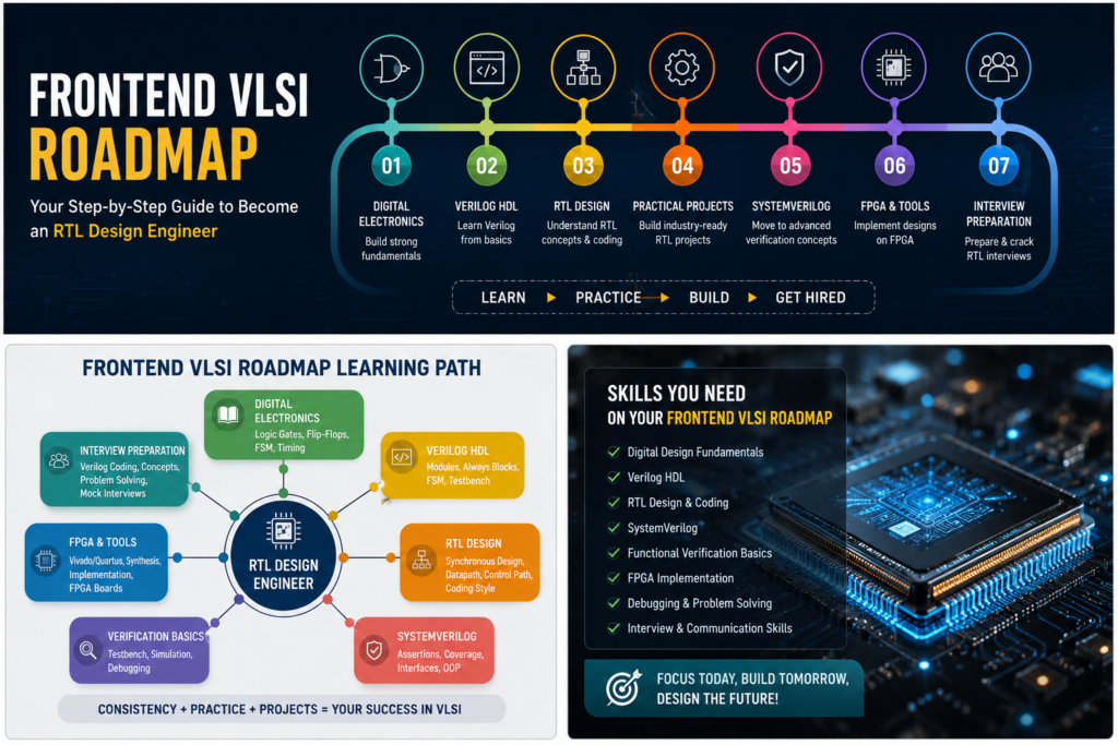
The semiconductor industry is experiencing unprecedented growth, creating exciting opportunities for aspiring engineers. If you are an ECE student, recent graduate, or professional looking to enter the chip design industry, understanding the Frontend VLSI Roadmap is the first step toward building a successful career as an RTL Design Engineer.

What Is the Frontend VLSI Roadmap?

Frontend VLSI focuses on designing and verifying digital circuits before they are physically implemented on silicon. Engineers in this domain work on RTL coding, functional verification, and architecture development using Hardware Description Languages (HDLs) such as Verilog and SystemVerilog.

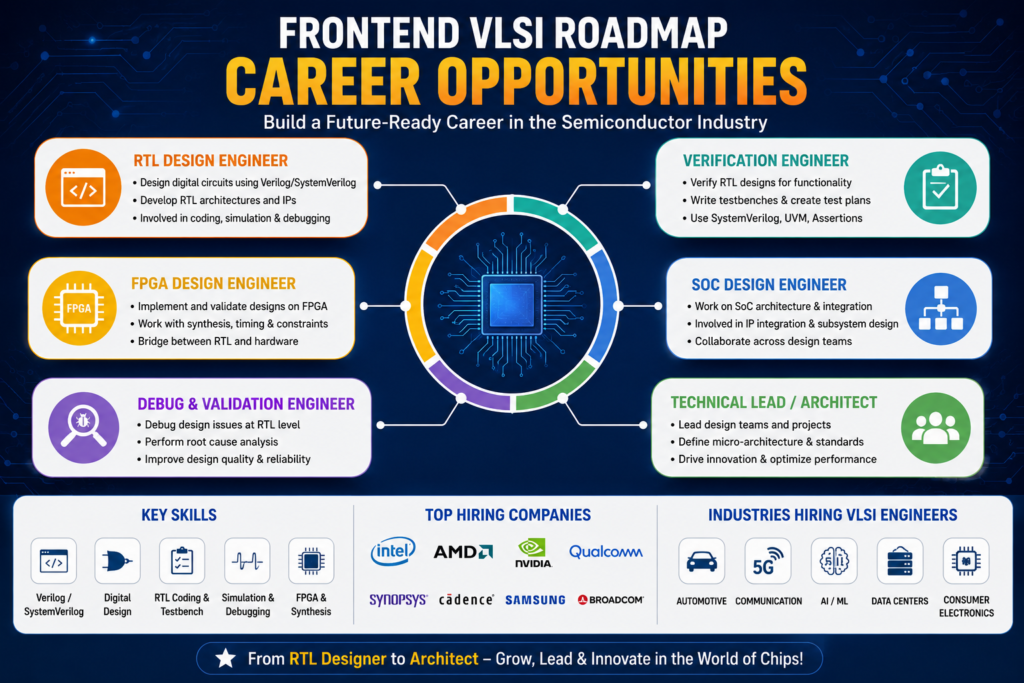
Popular frontend roles include:

  • RTL Design Engineer
  • Design Verification Engineer
  • FPGA Design Engineer
  • SoC Design Engineer

Frontend VLSI Roadmap Step 1: Learn Digital Electronics Fundamentals

Before jumping into RTL coding, you must build a strong foundation in digital electronics.

Key topics include:

  • Boolean Algebra
  • Logic Gates
  • Combinational Circuits
  • Sequential Circuits
  • Flip-Flops
  • Finite State Machines (FSMs)

A strong understanding of these concepts forms the foundation of every successful Frontend VLSI engineer.

Frontend VLSI Roadmap Step 2: Master Verilog HDL

Verilog is the backbone of RTL design. Every aspiring RTL engineer should become comfortable writing synthesizable Verilog code.

Focus on learning:

  • Modules and Ports
  • Always Blocks
  • Case Statements
  • Blocking vs Non-Blocking Assignments
  • FSM Coding
  • Testbench Development

Verilog proficiency is one of the most important milestones in the Frontend VLSI Roadmap.

Frontend VLSI Roadmap Step 3: Build Practical RTL Projects

Projects demonstrate your ability to apply concepts in real-world scenarios.

Recommended projects include:

Frontend VLSI Roadmap Project: Traffic Light Controller

Frontend VLSI Roadmap Project: UART Controller

Frontend VLSI Roadmap Project: FIFO Design

Frontend VLSI Roadmap Project: SPI Controller

These projects help develop RTL coding, debugging, and simulation skills that employers actively seek.

Frontend VLSI Roadmap Step 4: Learn SystemVerilog

Most semiconductor companies expect engineers to have working knowledge of SystemVerilog.

Important topics include:

  • Interfaces
  • Assertions
  • Functional Coverage
  • OOP Concepts

Learning SystemVerilog strengthens your position in the Frontend VLSI job market.

Frontend VLSI Roadmap Step 5: Prepare for RTL Design Interviews

Technical interviews typically focus on:

  • Digital Electronics
  • Verilog Coding
  • FSM Design
  • Timing Analysis
  • Setup and Hold Time
  • Debugging Scenarios

Interview preparation is a critical stage of the Frontend VLSI Roadmap.

Frontend VLSI Roadmap Career Opportunities

Engineers with strong RTL design skills are hired by semiconductor companies, product organizations, and technology startups.

Common career paths include:

  • RTL Design Engineer
  • Verification Engineer
  • FPGA Engineer
  • SoC Design Engineer

As experience grows, professionals can advance into architecture and technical leadership positions.

Why Following a Frontend VLSI Roadmap Accelerates Your Career

A structured learning path helps avoid common mistakes and ensures that you develop the skills employers demand. By mastering digital design, Verilog, SystemVerilog, RTL projects, and interview preparation, you can significantly improve your chances of landing your first VLSI role.

Conclusion: Start Your Frontend VLSI Roadmap Today

Following a structured Frontend VLSI Roadmap is one of the fastest ways to become job-ready in the semiconductor industry. With the right combination of technical knowledge, hands-on projects, and interview preparation, you can build a rewarding career as an RTL Design Engineer.

Ready to Accelerate Your Frontend VLSI Roadmap?

Join the VLSI Insights Frontend VLSI Program for expert mentorship, industry-level projects, interview preparation, and career guidance designed to help you become an RTL Design Engineer.

1. What is the Frontend VLSI Roadmap for beginners?

The Frontend VLSI Roadmap typically starts with Digital Electronics, followed by Verilog HDL, RTL Design, SystemVerilog, FPGA projects, and interview preparation. Following a structured roadmap helps students become job-ready RTL Design Engineers.

2. How long does it take to complete the Frontend VLSI Roadmap?

For most beginners, it takes around 6–12 months to become job-ready, depending on their learning pace, project experience, and interview preparation.

3. What skills are required to become an RTL Design Engineer?

The most important skills include:

  • Digital Electronics
  • Verilog HDL
  • RTL Design
  • FSM Design
  • SystemVerilog
  • Debugging and Simulation
  • Timing Concepts
  • Problem-Solving Skills

4. Is Verilog enough to get an RTL Design job?

Verilog is the foundation of RTL Design, but many companies also expect candidates to understand SystemVerilog, RTL verification basics, and industry-standard design practices.

5. Should I learn Verilog or SystemVerilog first?

You should start with Verilog because it forms the foundation of RTL Design. Once you are comfortable with Verilog, you can move on to SystemVerilog for advanced design and verification concepts.

6. Are FPGA projects important in the Frontend VLSI Roadmap?

Yes. FPGA projects help demonstrate practical implementation skills and strengthen your resume. Recruiters often prefer candidates who have worked on real-world projects such as UART, FIFO, SPI, or RISC-V processor designs.

7. What are the best projects for Frontend VLSI beginners?

Some of the best beginner-friendly projects include:

  • Traffic Light Controller
  • UART Controller
  • FIFO Design
  • SPI Controller
  • PWM Generator
  • Digital Clock

These projects help develop RTL coding, simulation, and debugging skills.

8. What is the average salary of an RTL Design Engineer in India?

The salary depends on experience and company type:

  • Freshers: ₹5–12 LPA
  • 2–5 Years: ₹12–25 LPA
  • 5+ Years: ₹25–50+ LPA

Professionals with strong RTL Design and SystemVerilog skills often receive higher compensation packages.

9. What interview topics are commonly asked for RTL Design roles?

Recruiters frequently ask questions on:

  • Digital Electronics
  • FSM Design
  • Verilog Coding
  • Blocking vs Non-Blocking Assignments
  • Setup and Hold Time
  • Clock Domain Crossing (CDC)
  • RTL Debugging

10. Is Frontend VLSI a good career in 2026?

Yes. The demand for Frontend VLSI engineers continues to grow due to advancements in AI, automotive electronics, 5G communication, data centers, and semiconductor manufacturing. RTL Design and Verification remain among the most sought-after skills in the industry.

11. Can ECE students start learning Frontend VLSI during college?

Absolutely. In fact, starting during college gives students an advantage because they can build projects, gain practical experience, and prepare for interviews before graduation.

12. What is the best way to learn Frontend VLSI?

The most effective approach is to combine:

  • Strong digital design fundamentals
  • Hands-on Verilog coding
  • Industry-level RTL projects
  • SystemVerilog training
  • Interview preparation

A structured training program with mentorship can significantly accelerate the learning process and improve job placement opportunities.

13. Which is the best Frontend VLSI course for freshers?

The best Frontend VLSI course should include Digital Electronics, Verilog, RTL Design, SystemVerilog, project-based learning, interview preparation, and placement assistance. Look for programs that provide hands-on industry projects and expert mentorship to help you become job-ready faster.

READ MORE-
https://community.cadence.com/cadence_blogs_8/b/di/posts/why-restructuring-matters-essential-insights-for-digital-design-engineers

Introduction

RTL Design interviews assess a candidate’s understanding of digital design, Verilog/SystemVerilog, timing concepts, finite state machines, protocols, and practical debugging skills.

This guide covers 50 commonly asked RTL Design interview questions that frequently appear in semiconductor companies.


Verilog and SystemVerilog Questions

1. What is RTL Design?

RTL Design describes hardware behavior using registers and data transfers between them.

2. Difference between Verilog and SystemVerilog?

SystemVerilog extends Verilog with advanced RTL and verification features.

3. Difference between blocking and non-blocking assignments?

Blocking (=) executes sequentially.

Non-blocking (<=) executes concurrently.

4. When should non-blocking assignments be used?

Sequential logic.

5. When should blocking assignments be used?

Combinational logic.

6. What is latch inference?

Occurs when combinational logic is incompletely specified.

7. What is synthesizable RTL?

RTL that can be converted into hardware gates.

8. Difference between wire and reg?

Wire represents connections.

Reg stores values.

9. What is an always_comb block?

SystemVerilog construct for combinational logic.

10. What is an always_ff block?

SystemVerilog construct for sequential logic.


FSM Questions

11. What is an FSM?

Finite State Machine controlling system behavior.

12. Difference between Moore and Mealy FSM?

Moore outputs depend on state.

Mealy outputs depend on state and inputs.

13. What is one-hot encoding?

Each state uses a dedicated flip-flop.

14. Why use FSM encoding?

Improves implementation efficiency.

15. What are common FSM interview mistakes?

Missing reset logic and unreachable states.


Timing Questions

16. What is setup time?

Minimum time before clock edge for stable data.

17. What is hold time?

Minimum time after clock edge for stable data.

18. What is clock skew?

Difference in clock arrival times.

19. What causes setup violations?

Long combinational paths.

20. What causes hold violations?

Excessively short paths.


CDC Questions

21. What is CDC?

Clock Domain Crossing.

22. Why is CDC important?

Prevents metastability issues.

23. What is metastability?

Unpredictable flip-flop behavior.

24. How is CDC handled?

Synchronizers and FIFOs.

25. What is a two-flop synchronizer?

Standard CDC synchronization method.


Protocol Questions

26. What is AXI?

Advanced eXtensible Interface.

27. Difference between AXI and APB?

AXI is high-performance; APB is low-complexity.

28. What is SPI?

Serial Peripheral Interface.

29. What is I2C?

Inter-Integrated Circuit protocol.

30. What is UART?

Universal Asynchronous Receiver Transmitter.


Design Questions

31–50

Cover topics including:

  • Counters
  • Shift Registers
  • FIFOs
  • Memory Design
  • Arbitration
  • Pipeline Design
  • Clock Gating
  • Reset Synchronization
  • Low-Power Design
  • Debug Methodologies
  • Synthesis Constraints
  • Assertions
  • Functional Coverage
  • Design Optimization
  • Resource Sharing
  • Bus Interfaces
  • Register Design
  • Parameterized Modules
  • Code Reusability
  • Silicon Debug
  • RTL Best Practices

Interview Preparation Tips

  • Master Verilog and SystemVerilog.
  • Practice FSM design daily.
  • Learn CDC thoroughly.
  • Understand timing concepts deeply.
  • Build RTL projects.
  • Review protocols regularly.

Conclusion

RTL Design interviews test both theoretical concepts and practical engineering skills. By mastering these 50 questions and building hands-on RTL experience, candidates can significantly improve their chances of securing Frontend VLSI roles in the semiconductor industry.

  1. ASIC Design Flow Explained

Introduction

Application-Specific Integrated Circuits (ASICs) power modern smartphones, AI accelerators, automotive systems, networking equipment, and data centers. Behind every successful chip lies a structured development process known as the ASIC Design Flow.

For students and engineers entering the semiconductor industry, understanding the complete ASIC design flow is essential because it connects all major VLSI domains, including RTL Design, Verification, Physical Design, Timing Analysis, and Manufacturing.

In this guide, we explain each stage of the ASIC design cycle from specification to tapeout.


What Is an ASIC?


ASIC Design Flow Explained.

An ASIC (Application-Specific Integrated Circuit) is a custom-designed semiconductor chip optimized for a specific application.

Examples include:

  • AI Accelerators
  • Smartphone Processors
  • Networking Switches
  • Automotive Controllers
  • SSD Controllers

Unlike general-purpose processors, ASICs are designed for dedicated functionality and optimized performance.

Asic design flow explained.


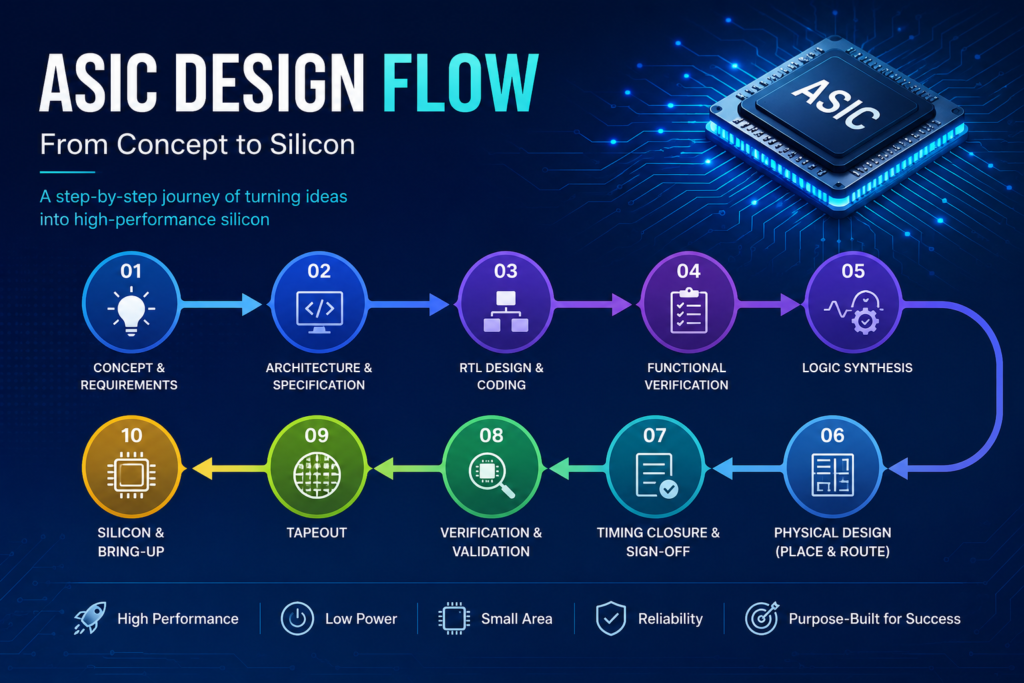
Overview of the ASIC Design Flow

The ASIC design flow consists of:

  1. Specification
  2. Architecture Design
  3. RTL Design
  4. Functional Verification
  5. Synthesis
  6. Design for Testability (DFT)
  7. Floorplanning
  8. Placement
  9. Clock Tree Synthesis
  10. Routing
  11. Static Timing Analysis
  12. Physical Verification
  13. Signoff
  14. Tapeout

Each stage contributes to ensuring the chip functions correctly and can be manufactured successfully.


1. Specification Phase

Every ASIC project begins with requirements gathering.

Engineers define:

  • Functional requirements
  • Performance targets
  • Power constraints
  • Area goals
  • Cost limitations

This document serves as the foundation for the entire project.


2. Architecture Design

System architects determine:

  • Processing blocks
  • Memory hierarchy
  • Bus interfaces
  • Pipeline structure
  • Clocking strategy

Architecture decisions have a major impact on performance and power consumption.


3. RTL Design

RTL engineers convert architecture into hardware description languages.

Common languages:

  • Verilog
  • SystemVerilog

RTL design includes:

  • FSM Development
  • Data Path Design
  • Protocol Controllers
  • Interface Logic

RTL is the heart of Frontend VLSI.


4. Functional Verification

Verification ensures RTL behaves according to specification.

Verification activities include:

  • Simulation
  • Assertions
  • Coverage Analysis
  • UVM Testbenches
  • Debugging

Verification often consumes over 60% of the design cycle.


5. Logic Synthesis

Synthesis converts RTL into gate-level netlists.

Goals:

  • Meet timing
  • Reduce area
  • Minimize power

Output:

  • Gate-Level Netlist

6. Design for Testability (DFT)

DFT improves manufacturing test coverage.

Common techniques:

  • Scan Chains
  • Boundary Scan
  • BIST
  • JTAG

DFT helps detect manufacturing defects.


7. Floorplanning

Backend engineers define:

  • Macro placement
  • Memory locations
  • Power grid
  • I/O placement

A good floorplan improves timing and routing efficiency.


8. Placement

Standard cells are positioned inside the chip area.

Objectives:

  • Minimize congestion
  • Improve timing
  • Optimize utilization

9. Clock Tree Synthesis (CTS)

CTS distributes clock signals across the chip.

Goals:

  • Reduce skew
  • Control latency
  • Improve timing reliability

10. Routing

Routing connects all placed cells using metal layers.

Routing must satisfy:

  • Timing constraints
  • Design rules
  • Signal integrity requirements

11. Static Timing Analysis (STA)

STA verifies timing without simulation.

Key checks:

  • Setup Time
  • Hold Time
  • Clock Skew
  • Timing Closure

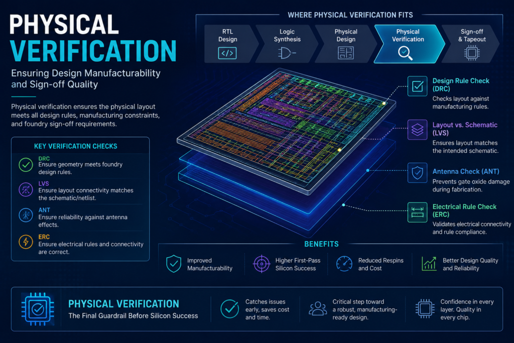
12. Physical Verification

ASIC Design Flow Explained.

Verification before manufacturing includes:

  • DRC
  • LVS
  • ERC

These checks ensure layout correctness.


13. Signoff

Signoff confirms:

  • Timing closure
  • Power integrity
  • Physical verification
  • Reliability metrics

Only signoff-approved designs proceed further.


14. Tapeout

Tapeout is the final stage.

Design data is sent to the semiconductor foundry for fabrication.

This marks the transition from design to manufacturing.


Career Opportunities Across the ASIC Flow

Frontend Roles:

  • RTL Design Engineer
  • Verification Engineer
  • FPGA Engineer

Backend Roles:

  • Physical Design Engineer
  • STA Engineer
  • DFT Engineer

System Roles:

  • SoC Engineer
  • Architecture Engineer

Conclusion

The ASIC design flow is a structured process that transforms a concept into silicon. Understanding each stage helps engineers appreciate how Frontend and Backend VLSI work together to build modern semiconductor products.

Whether your goal is RTL Design, Verification, Physical Design, or Architecture, mastering the ASIC flow provides the foundation for a successful VLSI career.

VLSI INSIGHTS -socials

Follow VLSI Insights linkedin https://www.linkedin.com/company/104170744/admin/page-posts/published/

follow Youtube – https://www.youtube.com/@VLSIInsights9

Follow Instagram – https://www.instagram.com/vlsiinsights/

Introduction

One of the most common questions asked by engineering students and fresh graduates entering the semiconductor industry is:

“Should I choose Frontend VLSI or Backend VLSI?”

Both domains are critical to chip development, and neither can exist without the other. However, for students who enjoy digital design, coding, problem-solving, and architecture development, Frontend VLSI often provides a broader technical foundation and long-term career flexibility.

In this article, we compare Frontend and Backend VLSI in detail, explore career opportunities, required skills, and explain why Frontend VLSI continues to attract many aspiring semiconductor engineers.


Understanding the VLSI Design Flow

The ASIC design cycle can broadly be divided into two major domains:

Frontend VLSI

Frontend focuses on:

  • Architecture Design
  • RTL Development
  • Verilog/SystemVerilog Coding
  • Functional Verification
  • CDC/RDC Analysis
  • Protocol Development
  • Simulation and Debugging

The goal is to ensure the design functions correctly before implementation.


Backend VLSI

Backend focuses on:

  • Floorplanning
  • Placement
  • Clock Tree Synthesis (CTS)
  • Routing
  • Static Timing Analysis (STA)
  • Physical Verification
  • Power Optimization

The goal is to convert RTL into a manufacturable silicon layout.


Frontend vs Backend VLSI Comparison

AreaFrontend VLSIBackend VLSI
Core FocusFunctionalityPhysical Implementation
LanguagesVerilog, SystemVerilogTCL, Shell
Main WorkRTL Design & VerificationPhysical Design & STA
Architecture ExposureHighLimited
Coding RequirementVery HighModerate
DebuggingExtensiveModerate
Silicon ImplementationLowHigh

Why Many Engineers Prefer Frontend VLSI

Frontend VLSI provides exposure to the logical behavior of a chip before it becomes silicon.

Engineers working in frontend gain experience in:

  • Digital design fundamentals
  • Processor architecture
  • Communication protocols
  • Verification methodologies
  • RTL development
  • Design debugging

These skills form the foundation of semiconductor engineering.


Advantage 1: Strong Design Fundamentals

Frontend engineers understand how hardware actually works.

They learn:

  • FSM Design
  • Data Path Design
  • Control Logic
  • Bus Protocols
  • Microarchitecture

This knowledge remains valuable throughout an engineer’s career.


Advantage 2: Greater Coding Exposure

If you enjoy programming and logic development, frontend is often more engaging.

Common technologies include:

  • Verilog
  • SystemVerilog
  • UVM
  • Python
  • Assertions (SVA)

Frontend engineers spend a significant portion of their time designing and debugging code.


Advantage 3: Easier Transition Into Specialized Domains

A strong frontend foundation can lead to careers in:

  • RTL Design
  • Design Verification
  • SoC Design
  • FPGA Development
  • AI Accelerator Design
  • CPU Design
  • Architecture Engineering

Many advanced semiconductor roles require deep frontend knowledge.


Advantage 4: Growing Demand for RTL and Verification Engineers

With the rise of:

  • AI Processors
  • Automotive Electronics
  • Edge Computing
  • Data Center Hardware

The demand for skilled RTL and Verification Engineers continues to grow.

Companies increasingly seek engineers who can develop complex digital systems efficiently.


When Backend VLSI Might Be a Better Choice

Backend VLSI can be an excellent fit if you enjoy:

  • Physical implementation
  • Timing closure
  • Layout optimization
  • Performance tuning
  • Manufacturing-focused challenges

Backend engineers play a critical role in turning designs into working silicon.


Skills Required for Frontend VLSI

To build a successful frontend career, engineers should focus on:

Core Skills

  • Verilog
  • SystemVerilog
  • Digital Design
  • FSM Design
  • Timing Concepts

Advanced Skills

  • UVM Verification
  • Assertions (SVA)
  • CDC Analysis
  • RDC Analysis
  • Protocol Verification

Additional Skills

  • Python Automation
  • Git
  • Linux
  • AI-Assisted Design Tools

Career Opportunities in Frontend VLSI

Popular job roles include:

  • RTL Design Engineer
  • Design Verification Engineer
  • FPGA Engineer
  • SoC Design Engineer
  • Formal Verification Engineer
  • Architecture Engineer

These roles often provide strong technical growth and opportunities to work on cutting-edge semiconductor products.


Learn Frontend VLSI with VLSI Insights

For students and professionals looking to enter the semiconductor industry, structured learning can significantly reduce the learning curve.

VLSI Insights offers Frontend VLSI training focused on industry-relevant skills such as:

  • Verilog
  • SystemVerilog
  • RTL Design
  • Functional Verification
  • UVM Fundamentals
  • CDC Concepts
  • Interview Preparation
  • Real-World Project Exposure

A structured roadmap helps engineers develop practical skills that align with industry expectations and improve their readiness for RTL Design and Verification roles.


Frequently Asked Questions

Is Frontend VLSI better than Backend VLSI?

Neither is universally better. However, Frontend VLSI is often preferred by engineers who enjoy coding, architecture, digital design, and verification.

Which domain has more coding?

Frontend VLSI generally involves significantly more coding through Verilog, SystemVerilog, UVM, and automation scripts.

Which is easier for beginners?

Many beginners find Frontend VLSI easier to understand because it starts with digital design concepts and hardware behavior before moving into physical implementation.

Can I switch from Frontend to Backend later?

Yes. A strong understanding of RTL and digital design can help engineers understand the complete chip design flow and transition into related domains.

Which domain has better long-term growth?

Both offer strong opportunities. Frontend VLSI often provides broader exposure to architecture, verification, and design development, which can open doors to multiple specialized career paths.


Conclusion

Frontend and Backend VLSI are both essential to semiconductor development. However, for engineers who enjoy digital design, coding, architecture, and problem-solving, Frontend VLSI offers an exciting and versatile career path.

By building strong skills in RTL Design, SystemVerilog, Verification, and modern design methodologies, engineers can position themselves for long-term success in the rapidly growing semiconductor industry.

For students starting their VLSI journey, Frontend VLSI often provides the strongest foundation for understanding how modern chips are designed, verified, and optimized before they reach silicon.

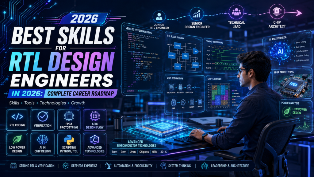
Introduction

Best Skills for RTL Design Engineers. – VLSI INSIGHTS

RTL (Register Transfer Level) Design remains one of the most sought-after career paths in the semiconductor industry. As modern chips become more complex and AI-driven applications continue to grow, companies are looking for engineers who possess a strong combination of digital design fundamentals, coding expertise, verification knowledge, and system-level understanding.

Whether you are a student, fresher, or experienced engineer looking to advance your career, understanding the skills that employers value most can significantly improve your opportunities in the VLSI industry.

In this article, we explore the most important skills every RTL Design Engineer should master in 2026.


What Does an RTL Design Engineer Do?

RTL Design Engineers are responsible for converting architectural specifications into synthesizable hardware descriptions using languages such as Verilog and System Verilog.

Their responsibilities typically include:

  • RTL coding
  • Microarchitecture development
  • Functional verification support
  • Timing-aware design
  • Power optimization
  • Design reviews and debugging

RTL design serves as the foundation of ASIC and SoC development.


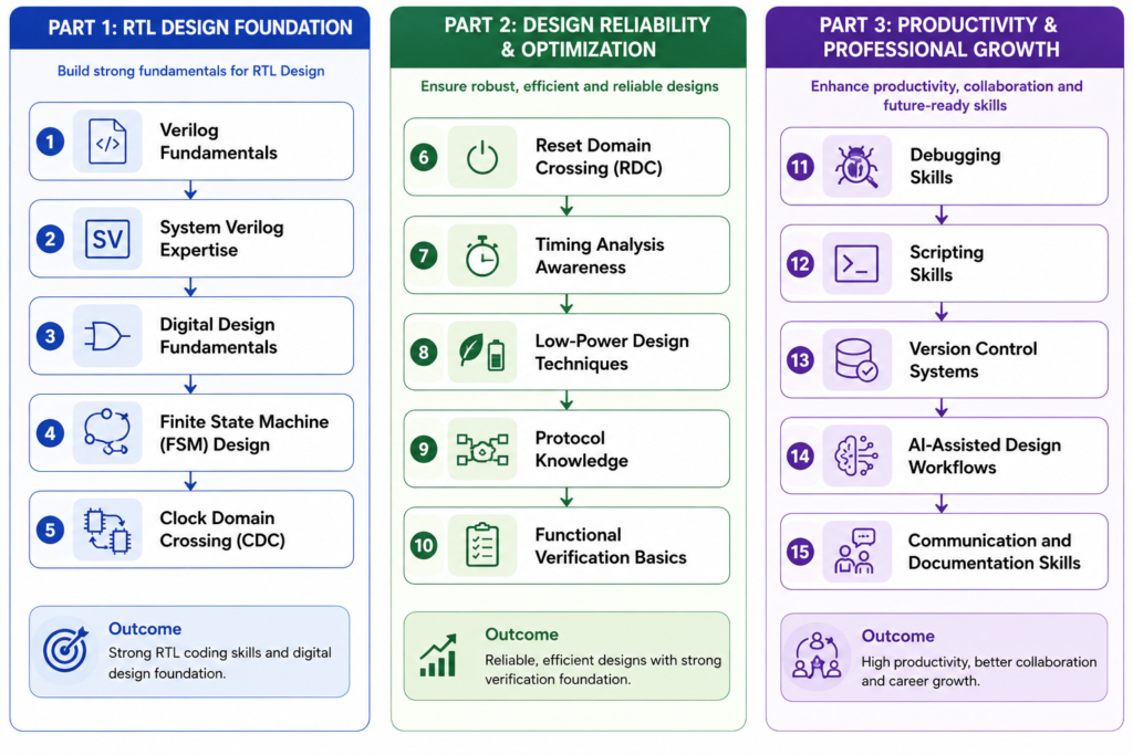
1. Verilog Fundamentals

Verilog remains one of the most important skills for RTL engineers.

Every engineer should understand:

  • Modules
  • Ports
  • Continuous assignments
  • Procedural blocks
  • Combinational logic
  • Sequential logic
  • Finite State Machines (FSMs)

Strong Verilog knowledge helps engineers write clean, synthesizable, and reusable RTL code.

Why It Matters

Most semiconductor companies still use Verilog extensively for RTL implementation and maintenance.


2. SystemVerilog Expertise

SystemVerilog has become the industry standard for modern RTL development.

Important concepts include:

  • always_comb
  • always_ff
  • always_latch
  • Interfaces
  • Packages
  • Enumerations
  • Structures
  • Assertions

SystemVerilog improves code readability, maintainability, and verification integration.

Industry Demand

Most leading semiconductor companies expect RTL engineers to have SystemVerilog experience.


3. Digital Design Fundamentals

A strong RTL engineer must understand digital electronics deeply.

Core concepts include:

  • Combinational circuits
  • Sequential circuits
  • FSM Design
  • Counters
  • Multiplexers
  • Encoders
  • Decoders
  • Arithmetic Logic Units

Without strong digital design knowledge, writing efficient RTL becomes difficult.


4. Finite State Machine (FSM) Design

FSM design is one of the most frequently tested topics in RTL interviews.

Engineers should know:

  • Moore FSM
  • Mealy FSM
  • State encoding
  • State optimization
  • One-hot encoding
  • Gray encoding

Why FSM Skills Matter

Most digital controllers are implemented using FSMs.

Examples include:

  • Protocol controllers
  • DMA engines
  • Bus interfaces
  • Communication modules

5. Clock Domain Crossing (CDC)

Modern SoCs contain multiple clock domains.

RTL engineers must understand:

  • Synchronizers
  • Metastability
  • CDC Violations
  • Asynchronous FIFOs
  • Handshake Synchronization

CDC issues can cause silicon failures if not handled properly.


6. Reset Domain Crossing (RDC)

RDC has become increasingly important in modern low-power designs.

Engineers should learn:

  • Reset synchronization
  • Reset sequencing
  • Asynchronous reset handling
  • RDC verification techniques

Many companies now include RDC checks in sign-off flows.


7. Timing Analysis Awareness

RTL engineers are not STA engineers, but they must understand timing concepts.

Important topics include:

  • Setup Time
  • Hold Time
  • Clock Skew
  • Clock Latency
  • Critical Paths

Timing-aware coding helps reduce backend challenges later in the design cycle.


8. Low-Power Design Techniques

Power efficiency is a critical requirement in modern chips.

Engineers should understand:

  • Clock Gating
  • Power Gating
  • Multi-Voltage Design
  • Retention Registers
  • Isolation Cells

Low-power design knowledge is highly valued in mobile, AI, and automotive applications.


9. Protocol Knowledge

Most RTL engineers work on standard communication protocols.

Common protocols include:

  • AXI
  • AHB
  • APB
  • PCIe
  • USB
  • Ethernet
  • I2C
  • SPI
  • UART

Protocol-related questions are common in interviews.


10. Functional Verification Basics

Although RTL and Verification are separate roles, RTL engineers benefit greatly from verification knowledge.

Useful skills include:

  • Testbench development
  • Assertions
  • Functional coverage
  • Debugging simulation failures

Understanding verification improves design quality and collaboration.


11. Debugging Skills

Debugging is one of the most valuable skills in semiconductor development.

Engineers should know how to:

  • Analyze waveforms
  • Trace signal paths
  • Identify root causes
  • Investigate simulation failures

Strong debugging skills often distinguish excellent engineers from average ones.


12. Scripting Skills

Automation is essential in modern chip development.

Recommended scripting languages:

  • Python
  • TCL
  • Shell Scripting

Automation helps improve productivity and reduce repetitive work.


13. Version Control Systems

Engineers should understand:

  • Git
  • Branching
  • Merging
  • Code Reviews

Version control is a standard requirement in professional design teams.


14. AI-Assisted Design Workflows

AI is becoming increasingly important in semiconductor design.

RTL engineers should learn:

  • AI-assisted code generation
  • Automated debugging
  • Design analysis tools
  • Prompt engineering for EDA workflows

Engineers who combine RTL expertise with AI knowledge will have a competitive advantage.


15. Communication and Documentation Skills

Technical knowledge alone is not enough.

Successful engineers can:

  • Explain design decisions
  • Participate in reviews
  • Create documentation
  • Collaborate effectively

Communication skills become increasingly important as engineers move into senior roles.


Top Skills Ranked by Industry Importance

  1. SystemVerilog
  2. Verilog
  3. Digital Design Fundamentals
  4. FSM Design
  5. CDC/RDC Analysis
  6. Timing Awareness
  7. Protocol Knowledge
  8. Debugging Skills
  9. Verification Basics
  10. Python/TCL Automation
  11. Low-Power Design
  12. AI-Assisted Design Workflows

Future of RTL Design Engineering

in this process of preparing for – Best Skills for RTL Design Engineers, The role of RTL engineers is evolving rapidly. While traditional RTL coding remains essential, future engineers will increasingly leverage AI-powered design tools, automation frameworks, and intelligent verification systems.

The engineers who succeed in 2026 and beyond will combine strong digital design expertise with automation, verification, and AI-driven workflows.


Conclusion

RTL Design Engineering continues to be one of the most rewarding and technically challenging careers in the semiconductor industry. Engineers who master Verilog, SystemVerilog, digital design fundamentals, CDC, timing awareness, and modern automation techniques will remain highly valuable in the years ahead.

Instead of focusing on a single skill, build a balanced foundation across design, verification, debugging, and automation. This approach will significantly improve both your interview performance and long-term career growth.

FAQs

  1. What skills are required for an RTL Design Engineer?
  2. Is System Verilog mandatory for RTL Design jobs?
  3. How important is CDC knowledge in RTL design?
  4. Do RTL engineers need Python programming?
  5. Can AI replace RTL Design Engineers?
  6. Which protocol is most important for RTL interviews?
  7. What is the salary of an RTL Design Engineer in India?
  8. How can freshers become RTL Design Engineers?

https://www.youtube.com/@VLSIInsights9

The semiconductor industry is evolving rapidly, driven by the explosive growth of Artificial Intelligence (AI), High-Performance Computing (HPC), cloud infrastructure, and edge devices. As demand for more powerful and efficient chips increases, traditional monolithic chip designs are reaching their physical and economic limits.

To overcome these challenges, semiconductor companies are increasingly adopting Chiplet Design—a revolutionary approach that breaks a large chip into multiple smaller dies called chiplets. This architectural shift is transforming how modern processors, AI accelerators, and data center chips are designed and manufactured.

In this article, we’ll explore what chiplets are, how chiplet-based design works, and why this technology is becoming one of the most important trends in the semiconductor industry in 2026.


A chiplet is a small semiconductor die designed to perform a specific function within a larger integrated system.

Instead of building a complete System-on-Chip (SoC) as one large piece of silicon, engineers divide the design into multiple specialized chiplets and connect them together inside a single package.

Each chiplet may handle a different function such as:

  • CPU Processing
  • Memory Control
  • Input/Output (I/O)
  • AI Acceleration
  • Graphics Processing

Together, these chiplets function as a single high-performance processor.


For decades, semiconductor companies relied on monolithic chip design, where all functions are integrated into a single silicon die.

While this approach has worked well, modern chips now contain billions of transistors, creating several challenges:

Advanced process nodes such as 3nm and 2nm require enormous investments in fabrication technology.

A defect anywhere on a large die can cause the entire chip to fail, increasing production costs.

Adding more functionality to a monolithic design becomes increasingly difficult as chip complexity grows.

These challenges have encouraged the industry to explore new design methodologies.


Chiplet-based design separates major functions into independent silicon dies.

A modern processor package may contain:

Contains processing cores and cache memory.

I/O Chiplet

Handles PCIe, USB, Ethernet, and external communication interfaces.

AI Accelerator Chiplet

Performs machine learning and AI computations.

Memory Chiplet

Provides high-speed memory access and storage functions.

These chiplets are connected through advanced packaging and high-speed interconnect technologies, allowing them to operate as a unified system.


Several industry trends are accelerating chiplet adoption.

1. The Rise of Artificial Intelligence

AI workloads require enormous computing power and memory bandwidth.

Chiplet architectures allow semiconductor companies to combine specialized compute engines, memory systems, and AI accelerators efficiently.

This flexibility makes chiplets ideal for AI-focused processors.

2. Better Manufacturing Efficiency

Smaller chiplets achieve higher manufacturing yields than large monolithic dies.

If one chiplet contains a defect, only that chiplet needs replacement instead of discarding the entire processor.

3. Faster Product Development

Chiplets can be reused across multiple product families.

A company can use the same I/O chiplet in desktop processors, server processors, and AI accelerators, significantly reducing development time.

4. Cost Optimization

Different chiplets can be manufactured using different process technologies.

For example:

  • CPU Chiplet → 3nm
  • I/O Chiplet → 7nm
  • Analog Chiplet → 14nm

This reduces manufacturing costs while maintaining performance.


Chiplets make it easier to increase processor performance by adding more specialized dies.

Higher Manufacturing Yield

Smaller dies have fewer defects and higher production success rates.

Lower Development Costs

Reusable chiplets reduce engineering effort and shorten product development cycles.

Better Performance per Dollar

Chiplets allow companies to achieve higher performance without dramatically increasing manufacturing costs.

Heterogeneous Integration

Different technologies can be integrated into a single package, creating highly optimized semiconductor solutions.


One of the biggest challenges in chiplet design is enabling fast communication between chiplets.

This is where UCIe (Universal Chiplet Interconnect Express) plays an important role.

UCIe is an industry-standard interconnect protocol designed to allow chiplets from different vendors to communicate efficiently.

Benefits of UCIe include:

  • High-speed communication
  • Lower latency
  • Vendor interoperability
  • Simplified chiplet ecosystem development

Many leading semiconductor companies are supporting UCIe as the future standard for chiplet connectivity.


Artificial Intelligence is currently the largest growth driver in the semiconductor industry.

Modern AI processors require:

  • Massive computational power
  • High-bandwidth memory
  • Efficient data movement
  • Scalable architectures

Chiplets enable designers to combine multiple AI accelerators, memory modules, and compute engines within a single package.

This approach improves:

  • Performance
  • Energy efficiency
  • Scalability

making chiplets essential for next-generation AI hardware.


As chiplet adoption increases, VLSI engineers will need to develop new skills.

Important areas include:

RTL Design

Developing reusable IP blocks that can function as independent chiplets.

Functional Verification

Verifying communication between multiple chiplets and subsystems.

System Architecture

Designing scalable multi-die semiconductor systems.

Advanced Packaging

Understanding 2.5D and 3D integration technologies.

High-Speed Interconnects

Working with standards such as UCIe and advanced communication protocols.

These skills are expected to become increasingly valuable in the coming years.


Despite its advantages, chiplet technology introduces new engineering challenges.

Interconnect Complexity

Communication between chiplets must be reliable, fast, and power efficient.

Verification Challenges

Multiple dies create additional validation and testing requirements.

Thermal Management

Packing several dies into a single package can generate significant heat.

Advanced cooling and packaging solutions are required to maintain performance and reliability.


Industry experts believe chiplets will become a standard design methodology for:

  • AI Accelerators
  • Data Center Processors
  • GPUs
  • Automotive Electronics
  • Edge Computing Devices
  • High-Performance Computing Systems

As AI applications continue expanding, chiplet-based architectures will play a critical role in delivering higher performance while controlling manufacturing costs.

The future of semiconductor innovation is no longer focused solely on shrinking transistors—it is increasingly focused on intelligently integrating specialized chiplets into powerful systems.


Conclusion

Chiplet design is transforming the semiconductor industry by providing a scalable, cost-effective alternative to traditional monolithic chips.

With benefits such as improved manufacturing yield, lower costs, better scalability, and support for AI workloads, chiplets are becoming a cornerstone of modern semiconductor architecture.

For students, engineers, and professionals working in VLSI and semiconductor design, understanding chiplet technology is becoming increasingly important as the industry moves toward a chiplet-driven future.


Frequently Asked Questions (FAQ)

What is a chiplet?

A chiplet is a small semiconductor die designed to perform a specific function within a larger chip package. Multiple chiplets work together to create a complete processor or system.

Why are chiplets important?

Chiplets improve manufacturing yield, reduce costs, and provide greater flexibility compared to traditional monolithic chip designs.

What is UCIe?

UCIe (Universal Chiplet Interconnect Express) is an industry-standard communication protocol that enables high-speed connectivity between chiplets.

Which companies are using chiplet technology?

Major semiconductor companies including AMD, Intel, NVIDIA, Broadcom, and TSMC are actively investing in chiplet-based architectures.

Are chiplets the future of semiconductor design?

Yes. Chiplets are widely considered one of the most important semiconductor innovations because they enable scalable, high-performance designs for AI, HPC, and next-generation computing applications.

Key Takeaways

  • Chiplets break large processors into smaller specialized dies for improved flexibility and scalability.
  • Chiplet-based design helps reduce manufacturing costs while improving production yield.
  • AI, data centers, and high-performance computing are accelerating chiplet adoption across the semiconductor industry.
  • UCIe is emerging as the key standard for high-speed communication between chiplets.
  • Major semiconductor companies such as AMD, Intel, NVIDIA, and TSMC are investing heavily in chiplet architectures.
  • Chiplet technology is expected to play a central role in the future of AI chips and next-generation semiconductor innovation.


The semiconductor industry is experiencing one of the biggest transformations in its history. With the rapid growth of Artificial Intelligence (AI), modern chip design is becoming more complex than ever before. From AI accelerators and high-performance processors to edge computing devices, today’s chips require billions of transistors and sophisticated design methodologies.

Traditionally, RTL design and verification have relied heavily on manual engineering effort. However, AI-powered Electronic Design Automation (EDA) tools are now helping engineers automate repetitive tasks, improve productivity, and reduce time-to-market.

This article explores how AI is changing RTL design and verification, what skills frontend engineers should develop, and what the future looks like for VLSI professionals.

What is RTL Design?

Register Transfer Level (RTL) design is the process of describing digital hardware behavior using Hardware Description Languages (HDLs) such as:

  • Verilog
  • System Verilog
  • VHDL

RTL acts as the bridge between system architecture and gate-level implementation.

Frontend engineers use RTL to:

  • Develop communication interfaces
  • Create memory controllers
  • Design processors
  • Build custom ASIC and SoC components

A well-written RTL design directly impacts Power, Performance, and Area (PPA).


Why AI is Entering the VLSI Frontend Flow

Modern chip designs contain:

  • Billions of transistors
  • Thousands of verification scenarios
  • Complex timing requirements
  • Multiple power domains

As design complexity increases, traditional manual workflows become difficult to scale.

AI helps by:

  • Generating RTL code
  • Identifying design bugs
  • Automating verification tasks
  • Predicting timing issues
  • Improving design space exploration

This significantly reduces engineering effort while increasing productivity.


AI Applications in RTL Design

AI-powered tools can generate Verilog or System Verilog code from natural language descriptions.

Example:

Input:

“Design a 16-bit synchronous up counter with asynchronous reset.”

AI can generate:

  • Module declaration
  • Counter logic
  • Reset logic
  • Testbench skeleton

This accelerates development and reduces coding effort.

  • Faster development
  • Reduced boilerplate coding
  • Improved productivity
  • Better documentation

AI tools can assist engineers in:

  • Pipeline planning
  • Resource allocation
  • Interface generation
  • Architecture tradeoff analysis

Instead of replacing engineers, AI acts as an intelligent design assistant.


AI models can analyze RTL code and identify:

  • Latch inference issues
  • Unreachable states
  • Coding violations
  • Potential timing bottlenecks

Finding bugs earlier reduces expensive redesign cycles later.


AI Applications in Verification

Verification often consumes nearly 70% of the overall chip design effort. This makes it one of the biggest opportunities for AI-driven automation.

AI can generate:

  • UVM environments
  • Sequences
  • Scoreboards
  • Coverage models

This reduces manual effort and speeds up project execution.


Coverage closure is one of the most time-consuming verification activities.

AI helps identify:

  • Coverage holes
  • Redundant tests
  • Missing scenarios

This allows teams to focus on high-value test cases.


Debugging simulation failures can take hours or days.

AI tools can:

  • Analyze waveforms
  • Trace root causes
  • Suggest fixes
  • Highlight suspicious signals

This dramatically reduces debug time.


Will AI Replace RTL Engineers?

The short answer is No.

AI can automate repetitive tasks, but it cannot fully replace:

  • Architecture decisions
  • Protocol understanding
  • System-level thinking
  • Silicon debugging
  • Performance optimization

Successful frontend engineers will use AI as a productivity tool rather than viewing it as competition.

The future belongs to engineers who can combine:

  • RTL expertise
  • Verification skills
  • AI-assisted workflows
  • System architecture knowledge

Skills Every Frontend Engineer Should Learn in 2026

To remain competitive, engineers should focus on:

  • Verilog
  • SystemVerilog
  • FSM Design
  • Low-Power Design
  • UVM
  • Assertions
  • Functional Coverage
  • Formal Verification
  • Clock Domain Crossing (CDC)
  • Reset Domain Crossing (RDC)
  • Timing Analysis
  • Power Optimization
  • Prompt Engineering for EDA
  • AI-Assisted Verification
  • AI-Based RTL Analysis
  • Intelligent Debug Tools

Career Opportunities

The growing semiconductor industry continues to create opportunities in:

  • RTL Design Engineering
  • Design Verification
  • FPGA Design
  • SoC Design
  • AI Hardware Development
  • EDA Tool Development

Professionals who understand both VLSI and AI will have a strong advantage in the coming years.


Challenges of AI in VLSI Design

Despite its benefits, AI still faces several limitations:

  • Hallucinated RTL code
  • Incomplete verification logic
  • Security concerns
  • Limited understanding of complex architectures

Human review remains essential before tape-out.


Future of VLSI Frontend Engineering

The next generation of chip design will likely involve:

  • AI-assisted RTL development
  • Automated verification environments
  • Intelligent design optimization
  • Agent-based EDA workflows
  • Faster design cycles

Rather than replacing engineers, AI will allow them to focus on higher-value engineering decisions.


Conclusion

Artificial Intelligence is rapidly transforming RTL design and verification workflows. Engineers who embrace AI tools can improve productivity, accelerate development cycles, and deliver better chip designs.

However, fundamental VLSI knowledge remains irreplaceable. Strong expertise in RTL design, verification methodologies, timing analysis, and system architecture will continue to be the foundation of a successful frontend engineering career.

The future of VLSI belongs not to AI alone, but to engineers who know how to leverage AI effectively.

Frequently Asked Questions (FAQ)

1. What is RTL design in VLSI?

RTL (Register Transfer Level) design is the process of describing digital circuit behavior using hardware description languages such as Verilog and System Verilog. It serves as the foundation for ASIC and FPGA development.


2. How is AI helping RTL designers?

AI assists RTL designers by generating code templates, detecting design issues, improving documentation, and automating repetitive design tasks. This allows engineers to focus more on architecture and optimization.


3. Can AI generate Verilog or System Verilog code?

Yes. Modern AI-powered tools can generate Verilog and System Verilog modules from natural language prompts. However, engineers must review and verify the generated code before implementation.


4. Will AI replace VLSI Frontend Engineers?

No. AI can automate routine tasks, but it cannot replace engineering judgment, architecture planning, protocol understanding, timing optimization, and silicon debugging. Engineers who use AI effectively will be more productive and valuable.


5. Which skills are most important for VLSI Frontend Engineers in 2026?

The most in-demand skills include:

  • Verilog
  • SystemVerilog
  • UVM Verification
  • Assertions (SVA)
  • Functional Coverage
  • CDC/RDC Analysis
  • Low-Power Design
  • AI-Assisted EDA Workflows

6. Is verification still important with AI tools available?

Absolutely. Verification remains the largest part of the chip design cycle. AI helps automate test generation and debugging, but engineers are still responsible for ensuring complete functional correctness.


7. What are the best career opportunities in VLSI Frontend Design?

Popular career roles include:

  • RTL Design Engineer
  • Design Verification Engineer
  • FPGA Engineer
  • SoC Design Engineer
  • Formal Verification Engineer
  • AI Hardware Engineer
  • EDA Tool Development Engineer

8. What is the future of AI in semiconductor design?

The future includes AI-assisted RTL generation, intelligent verification, automated debugging, design-space exploration, and agent-based EDA workflows that can significantly reduce chip development time.

Key Takeaways

  • AI is transforming RTL design and verification workflows.
  • Frontend engineers can use AI to improve productivity.
  • Verification remains critical despite automation advances.
  • System Verilog and UVM continue to be essential skills.
  • Engineers who combine AI knowledge with VLSI expertise will have stronger career opportunities in the semiconductor industry.